

Key Takeaways
- High frequency PCB manufacturing is essential for advanced electronics, ensuring reliable high-speed data transmission in applications such as 5G, satellite, and radar systems.
- Specialized materials like PTFE and ceramic-filled substrates are used to minimize signal loss and maintain dielectric stability above 500 MHz.
- Strict design and manufacturing processes—including impedance control, thermal management, and precise drilling—preserve signal integrity and prevent transmission errors.
- Common challenges such as signal loss and manufacturing costs are addressed through careful material selection, advanced inspection, and optimized fabrication processes.
- High frequency PCBs are critical for telecom infrastructure, aerospace, medical imaging, automotive radar, and IoT devices, powering the next generation of wireless technology.
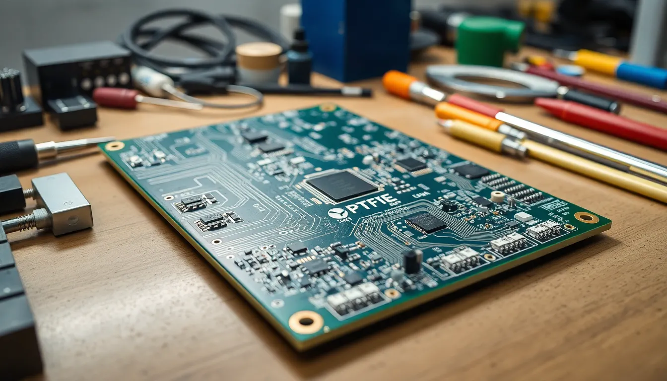
High frequency PCB manufacturing utilises specialised materials like PTFE and ceramic-filled substrates to ensure reliable signal transmission above 500 MHz for advanced electronics applications. These sophisticated boards require precise impedance control, thermal management, and strict manufacturing processes to minimise signal loss in demanding environments. Leading providers of high frequency pcb manufacturing services support critical applications across 5G infrastructure, aerospace systems, medical imaging equipment, and automotive radar technology.
Understanding High Frequency PCB Manufacturing
High frequency PCB manufacturing uses special materials and layout techniques to support reliable signal transmission above 500 MHz, including bands for 5G, satellite, and radar technologies. These PCBs depend on substrates like Rogers, Teflon (PTFE), and specialized FR-4, which lower signal loss and maintain electrical stability. Tight control over dielectric constant and dissipation factor prevents transmission errors as signal speed increases.
Manufacturers maintain strict tolerances for trace width, spacing, and layer registration. Laser direct imaging and precision drilling are standard steps for features under 100 μm. Automated Optical Inspection (AOI) checks ensure consistent circuit paths and via connections. Companies like OurPCB in China use high-frequency simulation, impedance control, and advanced laminating to match critical impedance values within ±10%.
Designs use microstrip and stripline structures with grounded shielding to limit electromagnetic interference. Standard stackups for these boards include 4–12 layers with high copper purity for stable current handling. These properties enable dependable high-speed performance in sectors like wireless communication, medical imaging, and aerospace systems, where signal clarity is a priority.
Key Materials Used in High Frequency PCBs
High frequency PCB manufacturing relies on materials engineered for signal integrity above 500 MHz. These substrate options address dielectric stability and thermal reliability, supporting telecom, aerospace, and wireless applications produced by suppliers like OurPCB.
PTFE-Based Laminates
PTFE-based laminates provide low dielectric loss and stable performance at frequencies above 1 GHz. These materials, including Teflon composites with fiberglass reinforcement, yield a dielectric constant around 2.2 and a loss tangent below 0.001 at 10 GHz. Strong chemical resistance and thermal stability make PTFE laminates common in 5G infrastructure and RF modules. OurPCB sources high-tolerance PTFE laminates for high-speed digital and analog designs, using strict handling and drilling processes to prevent surface defects and ensure reliable performance.
Ceramic-Filled Substrates
Ceramic-filled substrates deliver enhanced mechanical rigidity and better heat dissipation than standard PTFE, plus stable dielectric properties across temperature ranges. These materials feature dielectric constants between 3 and 10 and loss tangents under 0.003, suitable for radar or satellite receiver PCBs. This class reduces dimensional changes during processing, allowing tighter manufacturing tolerances. OurPCB integrates ceramic-filled options for customers requiring low-loss, high-frequency circuits in industrial control, medical imaging, and aerospace navigation, while optimizing for signal transmission and long-term reliability.
Critical Design Considerations
Critical design considerations in high frequency PCB manufacturing impact signal stability and system reliability. These considerations guide layout and material selection, as highlighted by production leaders like OurPCB.
Signal Integrity and Impedance Control
Signal integrity and impedance control determine performance in high frequency PCBs. Consistent impedance along traces, such as microstrip lines for RF circuits, reduces reflection and signal loss at frequencies above 500 MHz. Tight tolerance on trace width, spacing, and dielectric constant limits impedance variance to less than 10%. Material selection, including Rogers or PTFE substrates, maintains low dielectric loss for RF and 5G modules. OurPCB uses laser direct imaging to ensure precise registration and controlled impedance, verified by time-domain reflectometry (TDR) for quality assurance in communication, radar, and satellite designs.
Thermal Management
Thermal management safeguards device longevity in high frequency PCBs. Heat accumulation in dense RF circuits with PTFE or ceramic-filled substrates affects signal clarity and may degrade sensitive components in radar and medical applications. Metal-backed PCBs, thermal vias, and thick copper layers move heat away from critical parts. OurPCB integrates copper-filled thermal vias below high-power components to lower thermal resistance. Controlled laminate selection and board stack-up design manage heat dissipation across multilayer structures, supporting consistent RF system performance in telecom, aerospace, and industrial devices.
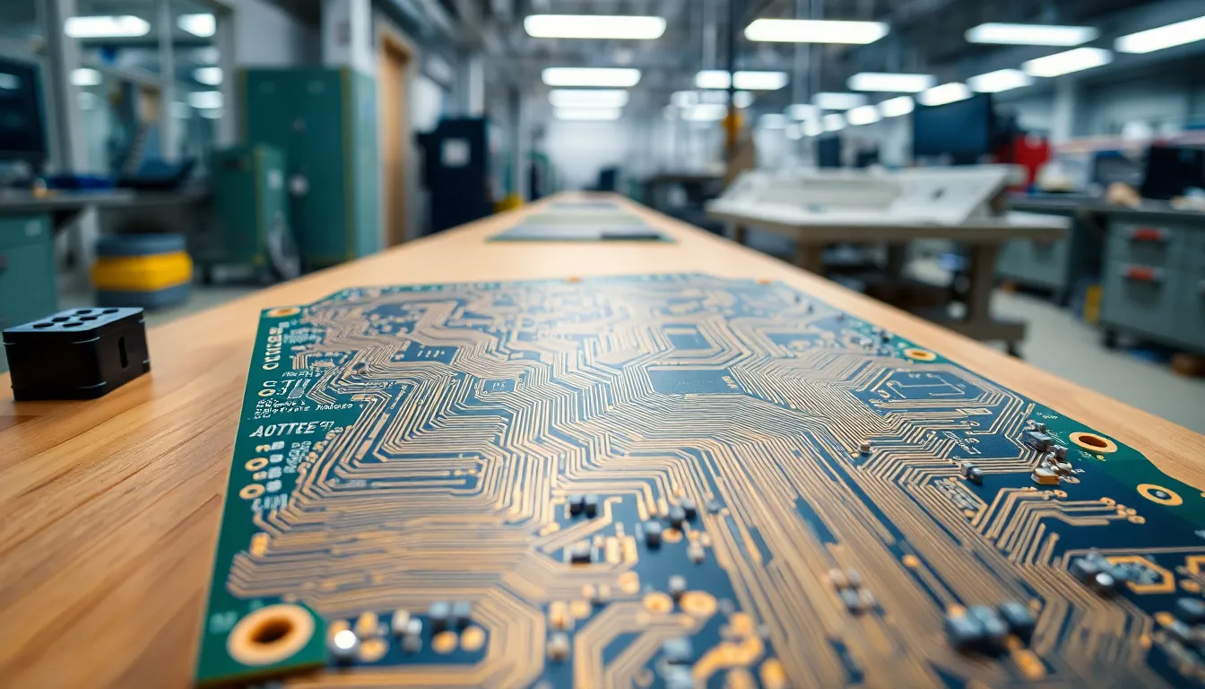
The High Frequency PCB Manufacturing Process
High frequency PCB manufacturing uses advanced techniques to maintain signal integrity and durability above 500 MHz. OurPCB applies industry-specific processes to deliver precise, reliable circuit boards for global clients in telecom, aerospace, and RF systems.
Layer Stack-Up and Lamination
Layer stack-up in high frequency PCB manufacturing defines signal paths and determines performance. OurPCB uses Rogers, PTFE, and high-speed FR-4 materials matched for dielectric consistency, thermal stability, and reduced signal loss. Engineers select the number and order of copper, prepreg, and core layers based on application requirements, such as 5G base stations or satellite modules. Lamination combines all layers under controlled heat and pressure, preventing air gaps that cause impedance discontinuity or signal distortion. Precision in this process helps maintain consistent impedance and minimizes crosstalk. For RF circuit boards, metal-backed stack-ups and additional ground planes are added to improve heat dissipation and electromagnetic shielding. Each step follows strict tolerances, confirmed by in-line electrical testing.
Precision Drilling and Plating
Precision drilling creates clean plated through holes (PTH) and microvias vital for multi-layer high frequency PCB performance. OurPCB uses CNC drilling with laser guidance to achieve hole diameters down to 0.1 mm for dense layouts, minimizing signal loss in high-speed lines. Routing and via placement adhere to minimum spacing rules to reduce parasitic inductance. The process includes laser microvia drilling for HDI designs required in phased array antennas or RF front ends. Copper plating deposits uniform conductive layers inside the drilled holes, critical for low resistance and reliable signal transmission. Panel-level inspection and Automated Optical Inspection (AOI) check for drill alignment, barrel integrity, and plating defects. These controls ensure that the finished high-frequency circuit boards handle the demands of next-generation wireless, radar, and medical imaging systems.
Common Challenges and Solutions
High frequency PCB manufacturing introduces unique production and design challenges. Manufacturers like OurPCB apply targeted solutions to minimize risk and improve board reliability across telecom and RF applications.
Minimizing Signal Loss
Minimizing signal loss in high frequency PCB manufacturing requires strict control of materials and fabrication steps. Engineers select low-loss substrates such as Rogers and PTFE to limit dielectric losses above 1 GHz. OurPCB maintains trace width tolerances within ±0.01 mm and enforces layer registration for consistent impedance, preventing reflection and crosstalk in high-speed signals like those in 5G systems. Microstrip and stripline configurations with grounded copper pour shield circuits from electromagnetic interference. Automated Optical Inspection (AOI) and TDR testing, performed during production at OurPCB, quickly detect deviations in critical traces, resulting in fewer failed boards and stable transmission for wireless and satellite designs.
Managing Costs and Yields
Managing costs and yields in high frequency PCB projects hinges on selecting suitable materials, optimizing panel use, and implementing precise fabrication controls. PTFE laminates guide higher costs, but their stable properties help avoid failures in radar or RF front-end modules, reducing costly redesigns. OurPCB uses CNC drilling and high-precision lamination to avoid defects like delamination or skewed microvias, maintaining high first-pass yields. Batch AOI and panel-level inspection ensure boards meet telecom and aerospace standards, reducing rework rates to below 2%. Customers benefit from predictable pricing and faster turnaround times, as streamlined processes minimize scrap and boost throughput during high-volume orders.
Applications of High Frequency PCBs
High frequency PCBs support essential functions in wireless communication, radar, and advanced imaging systems. These boards enable fast signal processing, data transfer, and low signal loss, maintaining reliable operation at GHz frequencies required for modern technology.
- 5G Base Stations and Infrastructure
Telecom companies use high frequency PCBs like those from OurPCB for 5G antennas, RF front-ends, and base station modules. These applications need stable performance above 3 GHz with close impedance control.
- Satellite and Aerospace Systems
Aerospace manufacturers specify PTFE or ceramic-filled PCB substrates for signal routing in satellites, radar, and avionics. OurPCB supplies boards for microwave communication and phased array radars, ensuring thermal stability and minimal delay.
- Medical Imaging Equipment
OEMs apply high frequency PCBs to MRI machines, wireless ultrasound, and RF probes. Boards from OurPCB guarantee low noise, stable impedance, and robust shielding for medical signal clarity.
- Automotive Radar and ADAS
Vehicle radar, collision avoidance, and advanced driver assistance systems (ADAS) rely on high frequency PCBs to support millimeter-wave sensors. OurPCB matches tight registration and dielectric specs for safety and accuracy.
- Industrial and IoT Wireless Devices
Designers integrate high frequency PCBs into IoT modules, point-to-point wireless links, and RF tags. OurPCB customizes multicore layouts for data networks, real-time tracking, and sensor integration.
Successful deployment in these applications results from strict signal control standards, advanced material choices, and precision manufacturing, core strengths of OurPCB’s high frequency PCB production.
About OurPCB
OurPCB is a leading provider of PCB manufacturing and assembly services, offering solutions such as turnkey PCB assembly, PCB design services, and rapid prototyping to bring your PCB concepts to life. Their comprehensive services cover everything from initial design consultation to final product delivery, ensuring high-quality printed circuit boards for various electronic applications. Whether it’s a simple prototype or a complex multi-layer PCB assembly, they are equipped to deliver reliable solutions for diverse electronic projects.
Contact:
Hommer Zhao, Owner
Phone: +1 626 790 1487
Email: [email protected]
Website: ourpcb.com
Location:
160 W Sierra Madre Blvd, Sierra Madre, CA 91024, USA
Frequently Asked Questions
What is a high frequency PCB?
A high frequency PCB is a specialized circuit board designed to handle signal transmission at frequencies above 500 MHz, crucial for advanced wireless, telecom, and radar applications. These boards use unique materials and design strategies to ensure reliable, high-speed data communication.
Why are high frequency PCBs important in modern electronics?
High frequency PCBs enable faster, smarter, and more reliable electronic devices. They are essential for applications like 5G networks, satellite communications, and advanced medical imaging, where signal clarity and speed are critical.
Which materials are commonly used in high frequency PCBs?
Common materials include PTFE (Teflon), Rogers laminates, ceramic-filled substrates, and high-speed FR-4. These materials offer low signal loss and stable dielectric properties, which are necessary for reliable high-speed performance.
What are the key design considerations for high frequency PCBs?
Designers focus on maintaining signal integrity, impedance control, and minimizing electromagnetic interference. Proper material selection, trace width/tolerances, and careful layer stack-up are essential to reduce reflection, signal loss, and crosstalk.
How do manufacturers ensure the quality of high frequency PCBs?
Manufacturers use advanced techniques like laser direct imaging, time-domain reflectometry (TDR), and Automated Optical Inspection (AOI) to ensure accurate trace layouts, clean drilled holes, and proper layer registration for high reliability.
What industries use high frequency PCBs?
High frequency PCBs are widely used in telecom (5G infrastructure), aerospace (satellite and radar), automotive (radar systems), medical imaging (MRI/CT scanners), and industrial IoT devices, where high-speed signal transmission is vital.
How do high frequency PCB materials affect performance?
Materials like PTFE and ceramic-filled substrates provide low dielectric loss, stable electrical performance, and good heat dissipation, all of which contribute to better signal integrity and durable, high-speed operation.
What challenges exist in manufacturing high frequency PCBs?
Challenges include minimizing signal loss, controlling manufacturing tolerances, managing costs, and maintaining high yields. Precision processing and strict quality control are needed to meet the demanding requirements of high frequency applications.
How is heat managed in high frequency PCBs?
Manufacturers use techniques such as metal-backed PCBs, thermal vias, and heat-dissipating substrates to manage heat efficiently, ensuring device longevity and consistent RF system performance.
What is the role of layer stack-up in high frequency PCB performance?
Proper layer stack-up and lamination are crucial for signal integrity in high frequency PCBs. The correct arrangement of materials prevents air gaps and controls impedance, reducing signal distortion and enhancing overall board reliability.